For sixty years the story of computing has been the same story told again. The transistor, the tiny switch that every chip is built from, gets smaller, so more of them fit in the same space, so the machine gets faster and cheaper. The switches are now so small that a few dozen of them would fit across a strand of DNA. That is also the problem. Silicon, the material the whole industry is built on, stops behaving like a good switch when it is sliced much thinner than it already is. The electrons start to leak.
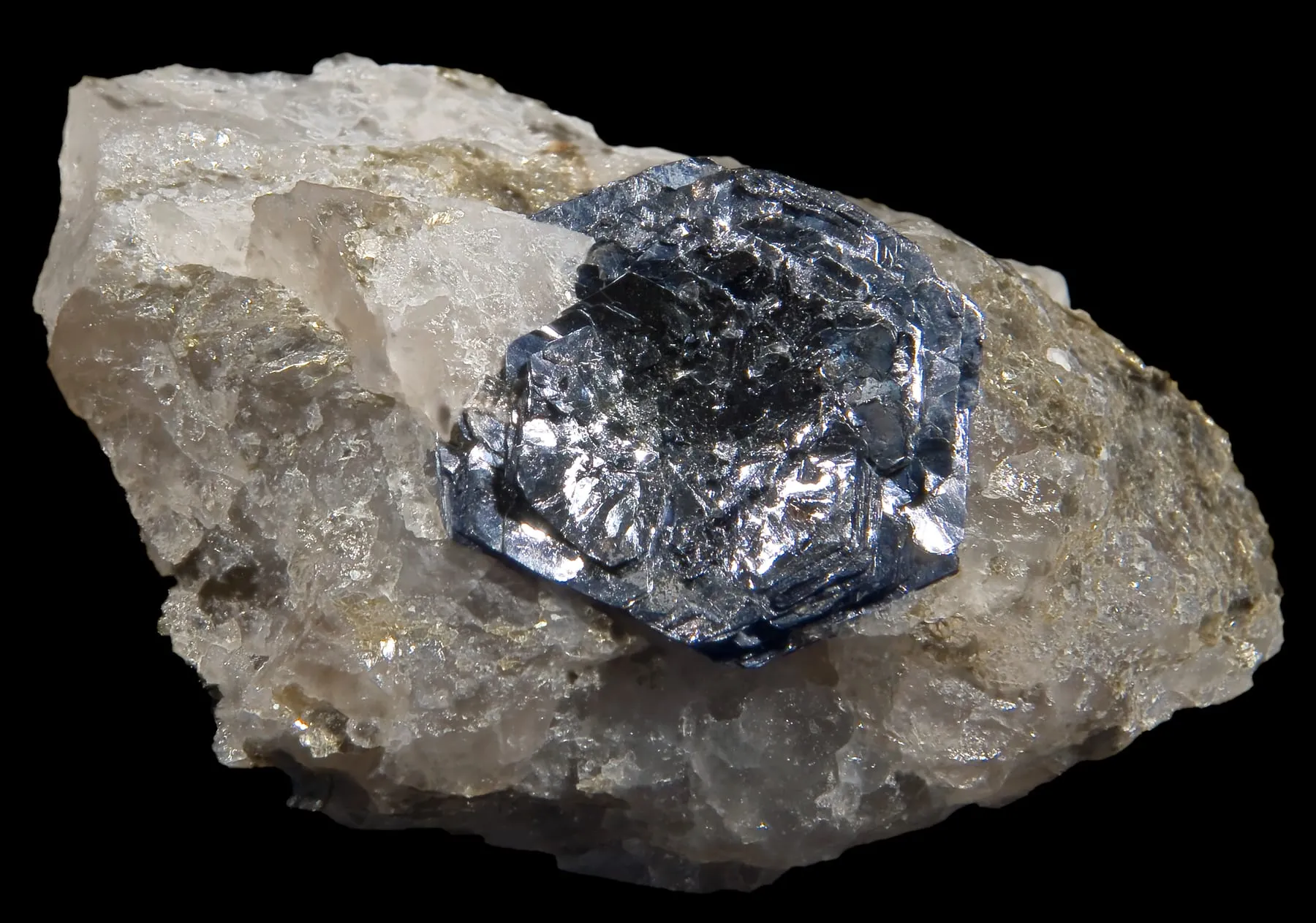
The crystal in the picture above is one of the leading candidates to take over when silicon runs out. It is molybdenite, the mineral form of molybdenum disulfide, and like graphite it peels into sheets. Peel it down far enough and you reach a single layer three atoms thick, a sheet so thin it is effectively two-dimensional. A channel that thin does not leak the way sliced silicon does, which is exactly why chip researchers have spent a decade trying to build transistors out of it.
The problem was never the channel
The trouble is that a transistor is not just its channel. Sitting on top of the channel is a thin layer of insulator called the gate, and it is the gate that does the actual switching. Push a voltage onto the gate and it reaches through the insulator to turn the current in the channel on or off. The thinner that insulating layer is, the more firmly the gate controls the channel, so thin is what you want.
Here is the bind. To lay a good insulator down on a normal chip, you rough up the surface first so the insulator has something to grip. On a channel that is three atoms thick, there is no surface to rough up without destroying the channel itself. Build the insulator directly onto the delicate two-dimensional sheet and you scar it, and a scarred channel carries a weak, sluggish current. For years the field faced a straight trade. You could have a thin insulator and tight control, or you could have a clean channel and good current, but not both.
A spacer made of near-nothing
The work that broke the trade came from National Yang Ming Chiao Tung University in Taiwan, working with the research arm of TSMC, the company that manufactures most of the world’s most advanced chips. Their answer, published in Nature Electronics, was to slip a buffer between the fragile channel and the insulator on top of it.
They grew an extremely thin layer of aluminium directly onto the molybdenum disulfide, so thin and so orderly that it followed the atomic pattern of the sheet beneath it. Then they let it oxidise, turning that aluminium into about 0.42 nanometres of aluminium oxide. A nanometre is a millionth of a millimetre, so this buffer is a couple of atoms deep, close to the thinnest a solid layer can meaningfully be. That near-nothing spacer gives the real insulator, a material called hafnium oxide, a smooth and continuous base to grow on, while shielding the channel underneath from the damage that used to ruin it.
What the numbers say
Two measurements tell you it worked. The first is that the finished gate stack behaves as though it were only about one nanometre thick, which is another way of saying the gate keeps a very firm grip on the channel. The second is a quantity called transconductance, which measures how sharply the current in the channel responds to a small nudge on the gate. It is the most honest single number for how good a switch you have built, and theirs came in at 0.45 millisiemens per micrometre, high for a two-dimensional device. A clean channel and a thin insulator, in the same transistor, at last.
The distance still left to run
It is worth being plain about what this is not. It is a single device in a laboratory, with a channel about a hundred nanometres long, which is enormous by the standards of a shipping chip. Nobody is going to buy a molybdenum disulfide processor next year, or the year after. A working transistor is a long way from a billion of them printed reliably on a wafer, and most promising results in this field have quietly stalled somewhere on that road.
What makes this one harder to wave off is where it came from. This is not only a university curiosity. TSMC does not publish on materials it has no intention of using, and the specific thing it solved here, getting a good insulator onto a two-dimensional channel without wrecking it, was one of the concrete reasons those channels were considered a decade away from a factory. Removing a known obstacle is not the same as arriving. It is how you find out whether the road goes through at all. For the first time in a while, the map past silicon has one fewer wall drawn across it.
Photograph: Didier Descouens, CC BY 3.0.